
The U.S. government is making a significant push to strengthen its semiconductor industry, announcing $1.5 billion in agreements with Amkor and SK Hynix under the CHIPS & Science Act. This investment aims to establish advanced chip packaging facilities within the United States, addressing a critical gap in the domestic supply chain.
Amkor's Arizona Expansion
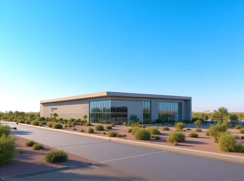
Amkor plans to construct a $2 billion advanced packaging facility near Peoria, Arizona, strategically located near TSMC's Fab 21. The agreement includes $400 million in direct funding and access to $200 million in loans under the CHIPS & Science Act. Apple is set to be Amkor's first and largest customer at this new facility. "This partnership underscores the facility's importance in strengthening the U.S. semiconductor supply chain," says a statement from Amkor.
The facility will occupy 55 acres and boast over 500,000 square feet of cleanroom space, significantly larger than Amkor's existing advanced packaging site in Vietnam. While specific capacity and technologies remain undisclosed, it is expected to cater to a wide range of industries, offering diverse packaging solutions like traditional, 2.5D, and 3D technologies. The project is anticipated to generate approximately 2,000 jobs, with operations scheduled to commence in 2027.
SK Hynix Invests in Indiana
SK Hynix has also signed a preliminary agreement with the U.S. government, receiving up to $450 million in direct funding and $500 million in loans to build an advanced memory packaging facility in West Lafayette, Indiana. 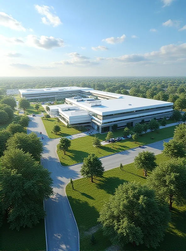 This facility, expected to begin operations in 2028, will assemble HBM4 and HBM4E memory. DRAM devices for high bandwidth memory (HBM) stacks will continue to be produced in South Korea, but packaging them in the U.S. is a major step forward. The potential to integrate these memory modules with high-end processors domestically is considered a significant development.
Beyond the packaging plant, SK Hynix plans to collaborate with Purdue University and other local research institutions to advance semiconductor technology and packaging innovations. This collaboration aims to boost research and development in the region, positioning the facility as a hub for AI technology and skilled employment.
These investments represent a crucial step in securing the U.S. semiconductor supply chain and reducing reliance on overseas manufacturing. By bringing chip packaging operations back to American soil, the government aims to foster innovation, create jobs, and maintain a competitive edge in the global technology landscape.

Broader Industry Trends
While these investments focus on packaging, other industry players are also making moves. Reports suggest that Broadcom and TSMC are independently exploring potential deals with Intel. These discussions are still preliminary, but reflect the ongoing shifts and strategic realignments within the semiconductor industry. Meanwhile, Samsung continues to dominate the global TV market, and LG leads in OLED TVs, showcasing the diverse strengths of different companies within the tech sector.
Recent reports also indicate some labor unrest at Samsung's Sriperumbudur plant in India, where workers protested the suspension of employees. This highlights the complexities and challenges that companies face as they expand their global operations.